In this section
Cost-Effective use of HDI PCB technology for SI, PI and EMC

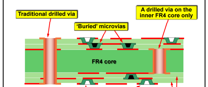
PCB manufacturing technology, also known as microvia technology, orSequential Build-Up technology (or simply ‘Build-Up’)uses ‘microvias’ 6 thou (0.15mm) diameter or less, socan achieve twice the number of pins/area than THPand which only connect between necessary board layers,so don’t constrain routing on other layers, all of which means they can significantly reducethe number of PCB layers requiredespecially where THP would require 10 layers or more.
You are free to use this information on condition that you do not modify it in any way and always make it clear who was its original author and where it was published or posted.Get more from EMC Standards
EMC Standards is a world-leading resource for all things EMC and EMI related. Our website is packed full of both free and paid-for content, including:
- Online quiz
- Webinars
- Training quiz
- And much more!

Electromagnetic Engineering (EMgineering) is the basis for proven good design practices for signal integrity (SI), power integrity (PI), and the control of EMI emissions and immunity (EMC).
Our aim is to help people learn how to more quickly and cost-effectively design and manufacture electronic equipment (products, systems, installations, etc.) to meet functional (i.e. SI/PI) specifications and conform to EMC standards, directives and other requirements.
Such equipment should benefit from reduced warranty costs and financial risks, whilst improving uptime, competitiveness and profitability.
We also cover basic good electrical safety engineering; and the Risk Management of Electromagnetic Disturbances / EMI, whether for Functional Safety or other types of risk.
Join EMC standards TODAY!